Introduction

In the world of electronics, understanding how to effectively place components on a printed circuit board (PCB) is crucial. The art and science of PCB component placement can make or break your project, influencing everything from performance to manufacturability. So, what is PCB component placement? At its core, it refers to the strategic positioning of various electronic components on a PCB layout to ensure optimal functionality.
Understanding the Basics of PCB Component Placement
PCB component placement involves more than just deciding where each part goes; it's about creating a harmonious design that balances electrical efficiency and thermal management. Knowing what does PCB mean in this context is essential for anyone involved in electronics design. When you consider how critical this process is, it's clear that proper PCB place design can lead to better performance and reliability in electronic devices.
Importance of Proper PCB Layout Design
The importance of proper PCB layout design cannot be overstated; it directly impacts the overall quality and longevity of electronic devices. A well-executed PCB place not only enhances signal integrity but also minimizes interference and heat generation, which are vital for device longevity. Moreover, understanding which country manufactures PCBs can give you insight into quality standards and production capabilities that influence your choices in sourcing these essential components.
Overview of PCB Component Placement Techniques
There are various techniques for effective PCB component placement that every designer should be aware of, from manual methods to sophisticated pcb place software solutions. These techniques help streamline the design process while ensuring that all components are placed accurately according to their electrical requirements and thermal characteristics. Additionally, utilizing a reliable PCB component placement machine can significantly enhance precision and speed in manufacturing processes—something every designer dreams about!
What is PCB Component Placement?

When diving into the world of electronics, one might wonder, What is PCB the place? In essence, PCB component placement refers to the strategic positioning of electronic components on a printed circuit board (PCB). This process is crucial because it influences how well the device performs and how efficiently it operates.
Defining PCB Component Placement
PCB component placement involves arranging various electronic parts—like resistors, capacitors, and integrated circuits—on a PCB according to specific design rules. Each component must be placed with precision to ensure optimal electrical connections and functionality. The art of pcb place design isn't just about aesthetics; it's about creating a reliable and efficient electronic layout.
Why It Matters in PCB Design
The importance of proper pcb place cannot be overstated; it directly impacts the overall performance of the circuit. Effective placement can reduce signal interference, enhance thermal management, and simplify assembly processes. Poorly executed placements can lead to malfunctions or even catastrophic failures in devices—making it essential for designers to prioritize this aspect during development.
Key Terms in PCB Placement
To navigate the realm of PCB component placement effectively, it's essential to familiarize yourself with some key terms. First up is footprint, which refers to the physical space that a component occupies on a PCB; understanding this helps in effective pcb place software usage. Another important term is clearance, indicating the minimum distance between components or traces to prevent short circuits—a vital consideration when determining where can PCBs be found within your design.
PCB Placement Design Principles

When diving into the world of PCB component placement, understanding the design principles is essential. Effective PCB layout hinges on a few fundamental concepts that ensure optimal performance and reliability. The right approach not only enhances functionality but also streamlines the manufacturing process, making it crucial for engineers to master these principles.
Fundamental Principles of Effective PCB Layout
At the heart of effective PCB layout design is the principle of organization. A well-structured layout minimizes signal interference and improves electrical performance, which is vital for any electronic device. Additionally, considering physical constraints such as size and shape can significantly impact how components are arranged on your board—this is where pcb place design shines.
Another key principle involves maintaining proper spacing between components to avoid potential short circuits or thermal issues. This leads us to another vital aspect: ensuring that high-frequency components are placed with care to reduce electromagnetic interference (EMI). Understanding What does PCB mean? in this context helps clarify why these principles are not just theoretical—they're practical guidelines that influence real-world applications.
Importance of Component Proximity
Component proximity plays a pivotal role in PCB design, affecting both electrical performance and manufacturability. When designing a circuit board, placing related components close together can minimize trace lengths, which reduces resistance and inductance—both critical for high-speed signals. So when asking Where can PCBs be found? remember they thrive in environments where component proximity is optimized.
However, it’s not just about cramming parts together; thoughtful placement can enhance thermal management as well. Components that generate heat should be spaced appropriately to allow for adequate airflow or cooling solutions. Thus, mastering component proximity can significantly influence the longevity and efficiency of your final product.
Impact of Electrical and Thermal Considerations
Electrical considerations are paramount in ensuring that your PCB functions correctly under various conditions. This includes understanding how voltage drops across traces can affect performance—a crucial factor when determining What is PCB the place? in terms of electrical integrity during operation. Poor placement decisions can lead to unwanted resistive losses or even catastrophic failures.
Thermal considerations cannot be overlooked either; excessive heat buildup can damage sensitive components over time if not properly managed through strategic placement and adequate spacing strategies. Using tools like pcb place software allows designers to simulate thermal behavior before finalizing their designs, thus preventing costly mistakes later on.
In summary, adhering to sound design principles regarding component placement will yield significant dividends throughout a PCB's lifecycle—from initial concept through manufacturing to end-user satisfaction.
PCB Placement Software Options

In the fast-paced world of electronics, having the right tools for PCB design can make all the difference. Choosing the best PCB place software is essential for achieving an efficient and effective layout. With numerous options available, understanding what makes a software package stand out can help you streamline your PCB component placement process.
Popular PCB Design Software
Tools like Altium Designer, Eagle, and KiCad have carved out significant niches in the market due to their robust features and user-friendly interfaces. Additionally, these platforms are widely recognized for their ability to handle complex designs while providing intuitive workflows that simplify what is otherwise a challenging task.
These popular options also cater to various levels of expertise; whether you’re a novice or a seasoned pro, there's something for everyone in this mix. Altium Designer is often favored by professionals for its advanced capabilities, while KiCad offers an open-source solution that appeals to hobbyists and startups alike. If you're wondering What does PCB mean? in terms of software applications, these platforms are prime examples that illustrate how digital tools can enhance traditional design methods.
Features to Look For in PCB Software
Choosing the right PCB place design software involves looking at several key features that enhance usability and efficiency. First off, intuitive design interfaces allow users to navigate easily through complex layouts without feeling overwhelmed—after all, who wants to wrestle with clunky software? Moreover, features like real-time DRC (Design Rule Checking) help catch errors before they become costly mistakes during production.
Another important aspect is simulation capabilities; being able to visualize how components will interact under various conditions can save time and resources later on. Additionally, libraries containing pre-defined components streamline the placement process by allowing designers quick access to commonly used parts—perfect when you're racing against deadlines! Ultimately, when searching for which country manufactures PCB? remember that good software can significantly impact where your designs end up being produced.
How Software Enhances Placement Efficiency
The right pcb place software not only simplifies the initial stages of design but also enhances overall placement efficiency throughout the project lifecycle. Automation features within these tools allow repetitive tasks such as component placement or routing to be completed with minimal manual input—talk about saving precious time! By optimizing workflows and reducing human error potential during placements, designers can focus on more creative aspects of their projects rather than getting bogged down by tedious details.
Additionally, collaboration features enable teams across different locations to work together seamlessly on designs—a must-have in today’s globalized environment where PCBs are often manufactured far from where they're designed. As you explore Where can PCBs be found? keep in mind that effective use of modern software plays a crucial role in ensuring your designs meet industry standards while maximizing productivity from concept through production phases.
The Role of PCB Component Placement Machines

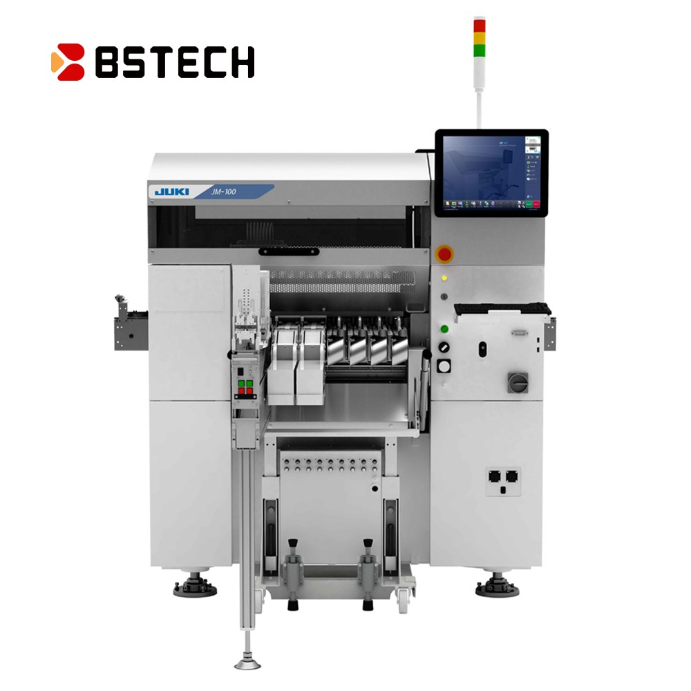
In the world of PCB design, the role of PCB component placement machines cannot be overstated. These sophisticated machines automate the process of placing components onto printed circuit boards with precision and speed. By understanding what these machines do, designers can enhance their workflow and improve overall product quality.
Overview of PCB Component Placement Machines
PCB component placement machines are specialized devices designed to accurately position electronic components on a PCB during manufacturing. Often referred to as pick-and-place machines, they utilize advanced technology to ensure components are placed in their designated spots with minimal human intervention. Understanding how these machines operate is crucial for anyone involved in PCB place design, as they significantly affect production efficiency and accuracy.
Benefits of Automated Placement
The benefits of automated placement using PCB component placement machines are numerous and impactful. First off, automation drastically reduces the time required for assembly, allowing manufacturers to ramp up production without sacrificing quality. Additionally, these machines minimize human error—an essential factor when you consider that even a tiny misplacement can lead to significant functional issues in PCBs.
Moreover, using automated systems allows for greater consistency in the manufacturing process; every board is assembled with the same level of precision regardless of who or what is operating the machine. This consistency is vital when producing large batches where even slight variances can lead to costly defects or failures down the line. In short, if you're wondering what does PCB mean in terms of efficiency and reliability, look no further than these automated solutions.
Leading Manufacturers of PCB Placement Equipment
Companies like Yamaha Motor Corporation and ASM Assembly Systems have established themselves as leaders by providing high-quality pcb place software along with their advanced machinery solutions. These manufacturers offer a range of options tailored for various production scales—from small startups needing flexibility to large enterprises requiring high-speed assembly lines.
Additionally, companies such as Juki Automation Systems and Panasonic provide robust options that cater specifically to different types of PCBs and components used across various industries globally—making them popular choices among those asking Which country manufactures PCB? Their cutting-edge technology ensures that users benefit from innovations designed specifically for modern-day challenges in electronics manufacturing.
In conclusion, understanding the role of PCB component placement machines is essential for anyone involved in electronic design or manufacturing processes today. With benefits ranging from increased efficiency to reduced errors and leading manufacturers offering top-notch solutions worldwide, investing in such technology can significantly enhance your overall production capabilities while ensuring high-quality outcomes across all projects.
Common Mistakes in PCB Component Placement

Identifying Frequent PCB Placement Errors
One of the most prevalent issues is inadequate spacing between components, which can lead to signal interference or thermal problems. Another error often seen in PCB place design is neglecting the layout's flow, causing unnecessary complexity and potential bottlenecks in signal routing. Additionally, failing to consider component orientation may result in assembly difficulties during manufacturing, making it vital to pay attention to every detail when determining what is PCB the place?
Consequences of Poor Placement Decisions
The repercussions of poor placement decisions can be severe, impacting both performance and reliability. For instance, if components are too close together without proper thermal management, overheating may occur—leading to premature failure or reduced lifespan of the device. Moreover, inefficient layouts can complicate troubleshooting and repairs down the line; this becomes especially problematic when considering which country manufactures PCB for specific applications.
Tips for Avoiding Mistakes
To steer clear of these pitfalls, one must prioritize careful planning and utilize effective pcb place software that aids in visualizing component relationships before finalizing designs. Regularly reviewing industry best practices can also help ensure all bases are covered when placing components on a board; asking questions like What does PCB mean? can clarify doubts regarding standards and expectations within your designs. Lastly, leveraging advanced tools like a PCB component placement machine allows for precision that manual placements simply can't achieve—making your design process smoother and more efficient.
Conclusion
In the world of electronics, understanding PCB component placement is crucial for creating efficient and reliable devices. As we wrap up, it’s essential to highlight best practices that can elevate your PCB design game and ensure your projects are successful. From utilizing the right software to avoiding common pitfalls, let’s dive into how you can enhance your PCB place endeavors.
Best Practices for PCB Component Placement
Effective PCB place design begins with a clear understanding of your circuit's functionality and layout requirements. Ensure that components are placed logically, minimizing trace lengths while considering electrical and thermal performance. Prioritizing component proximity can significantly reduce interference and improve signal integrity, making it vital to think about how each part interacts within the overall design.
When exploring what is PCB placement? it's all about strategic organization—components should be arranged in a way that facilitates easy assembly and maintenance. This means considering access points for soldering and ensuring that larger components don’t obstruct smaller ones during assembly or repair work. Additionally, employing advanced PCB place software can streamline the process by providing visual aids and simulation tools to optimize placement before manufacturing.
Where to Find Quality PCB Components
Finding quality components is as important as mastering the art of placement itself; after all, what does PCB mean if not built with reliable parts? Many manufacturers offer extensive catalogs online where you can browse through various options tailored to every need—from resistors to integrated circuits. Countries like China, Germany, and the United States are known for their robust electronics manufacturing sectors; thus, sourcing from reputable suppliers in these regions can yield high-quality PCBs.
You might wonder where can PCBs be found? Online marketplaces often serve as great starting points for sourcing components at competitive prices while also providing customer reviews for additional assurance of quality. Always verify supplier credentials before making purchases; a little research goes a long way in ensuring you’re using top-notch parts in your designs.
How Bensun Technology Can Help You
Bensun Technology stands out as an industry leader when it comes to offering comprehensive solutions for those diving into the world of PCB component placement machines and software tools. Their innovative products are designed not only to enhance efficiency but also to minimize errors during the assembly process—perfect for both beginners and seasoned professionals alike!
With Bensun’s expertise in pcb place technology, they provide tailored support that includes everything from initial design consultation through production assistance, ensuring you get exactly what you need without unnecessary hassle. By leveraging their state-of-the-art equipment alongside professional guidance, you're setting yourself up for success in every project you tackle.
